RSA SecurID hardware token reverse engineering
Reverse engineering an RSA SecurID hardware token to understand its key operation principles and how resistant they are to attacks to obtain the seed vs the software token option.
Hardware tokens vs Software tokens
At work we regularly have the discussion on whether we should introduce the convenient two-factor authentication software tokens to replace the physical RSA SecurID hardware tokens that we all carry around. The outcome of the review is nearly always that software tokens are good and convenient, but they are not as tamper proof / tamper evident as hardware tokens: it does not take much to steal the seed from a general purpose CPU and OS, it can be done without leaving any trace that the seed has been compromised, you do not need physical access to the device - effectively cloning the software token without the user knowledge and completely removing one of the factors.
To be fair it is relatively easy to reverse engineer the soft tokens and point out their flaws, while on the other side we just take RSA’s word at face value when they say that the hardware tokens are tamper resistant.
So, is it really that difficult to steal the seed from a SecurID hardware token or are we just relying on security through obscurity? Let’s find out…
Hardware token theory of operation
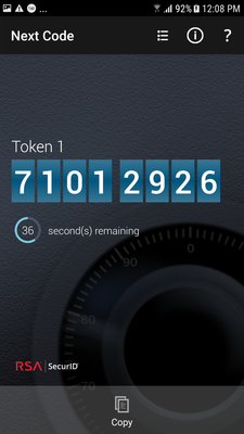
Without going too much into detail on how SecurID works, suffice to say that the token and the authentication server are time synchronised and share a secret (the seed). Using the current time and the seed, they use a non-reversible algorithm (older versions used an RSA proprietary algorithm but recent versions have moved to AES) to compute a 6-digit number. This number changes every minute and is not predictable, so it is used by a client to prove to the server that they are in physical posession of the token (the “something you have” factor).
Based on how the SecurID system operates let’s try to make a first guess on how the various components are implemented. For our analysis we are using the SecurID SID700 token, easily the most widely deployed RSA token.
Power
RSA tokens are purchased with a certain pre-programmed lifespan of 2 to 5 years: the longer the lifespan the more the token costs. When you receive a new token after purchase it is already showing token codes every minute, as a matter of fact the token does not have an “off” switch or a “show me my token code” button, it is simple and easy to use: the user just looks at the token and types the number they see.
The tokens are self-contained and are non-rechargeable, the battery that powers the whole system needs to last up to 5 years of continuous operation so this means that the implementation will focus on ultra-low current consumption.
Time synchronisation
While it is easy to keep synchronisation on the server-side, the tokens are totally self-contained so they must include a really accurate oscillator that does not drift substantially over the 3-5 years of token lifetime. The token will be imprinted with the timestamp when it is initialised and will keep track of the number of oscillations since then. The server will need to know, for each token, the time when it was initialised so it can work in sync.
Seed management
When you buy a batch of tokens, you also receive a “seed file” which needs to be loaded into the authentication server. There is nothing for you to do to the tokens, e.g. they come preloaded with the seeds and already showing valid numbers, the only thing you need to do is to assign a token to a user, and they are ready to go.
This means that, at some point in time, a random seed was generated and programmed into the token, the “imprint time” recorded and incorporated into a database at RSA which includes:
- Token serial
- Activation timestamp
- Seed
When somebody purchases a batch, the tokens are shipped from a warehouse and the corresponding database entries are sent to the customer as part of the “seed file”. At this point of time there is no need for RSA to keep a copy of the seeds, however it seems that they actually do keep the seeds after that as highlighted in the 2011 compromise of the RSA SecurID seed database. A good example on how retaining information beyond the point it ceases to be useful is a bad practice and just increases your exposure to attacks.
What would be your guess if you had to venture a reason why they kept a copy of the token seeds?
Updated Dec’2022: Mihai commented on this point (thanks!) and put forward the proposal of RSA keeping a copy of the seeds for customers who lose them, and they may not be too far off: an article published 10 years after the hack reveals the following nugget of information: “Even after the CD was shipped to a client, those seeds remained on the seed warehouse server as a backup if the customer’s SecurID server or its setup CD were somehow corrupted.”
Token manufacture
Because the token arrives with the seed preloaded it needs to be programmed before it gets to us.
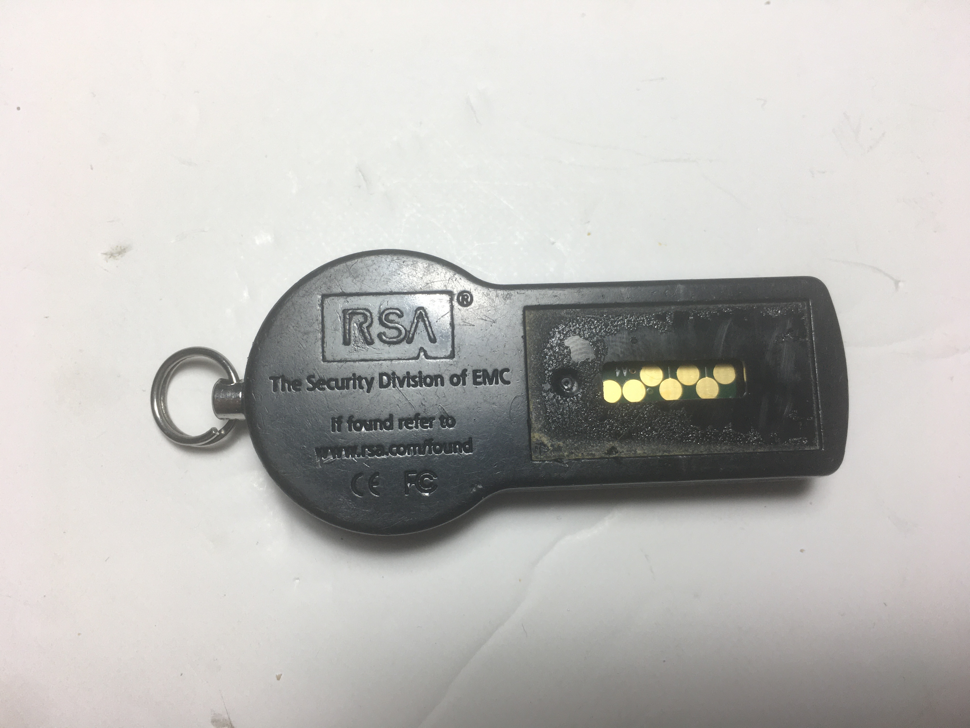
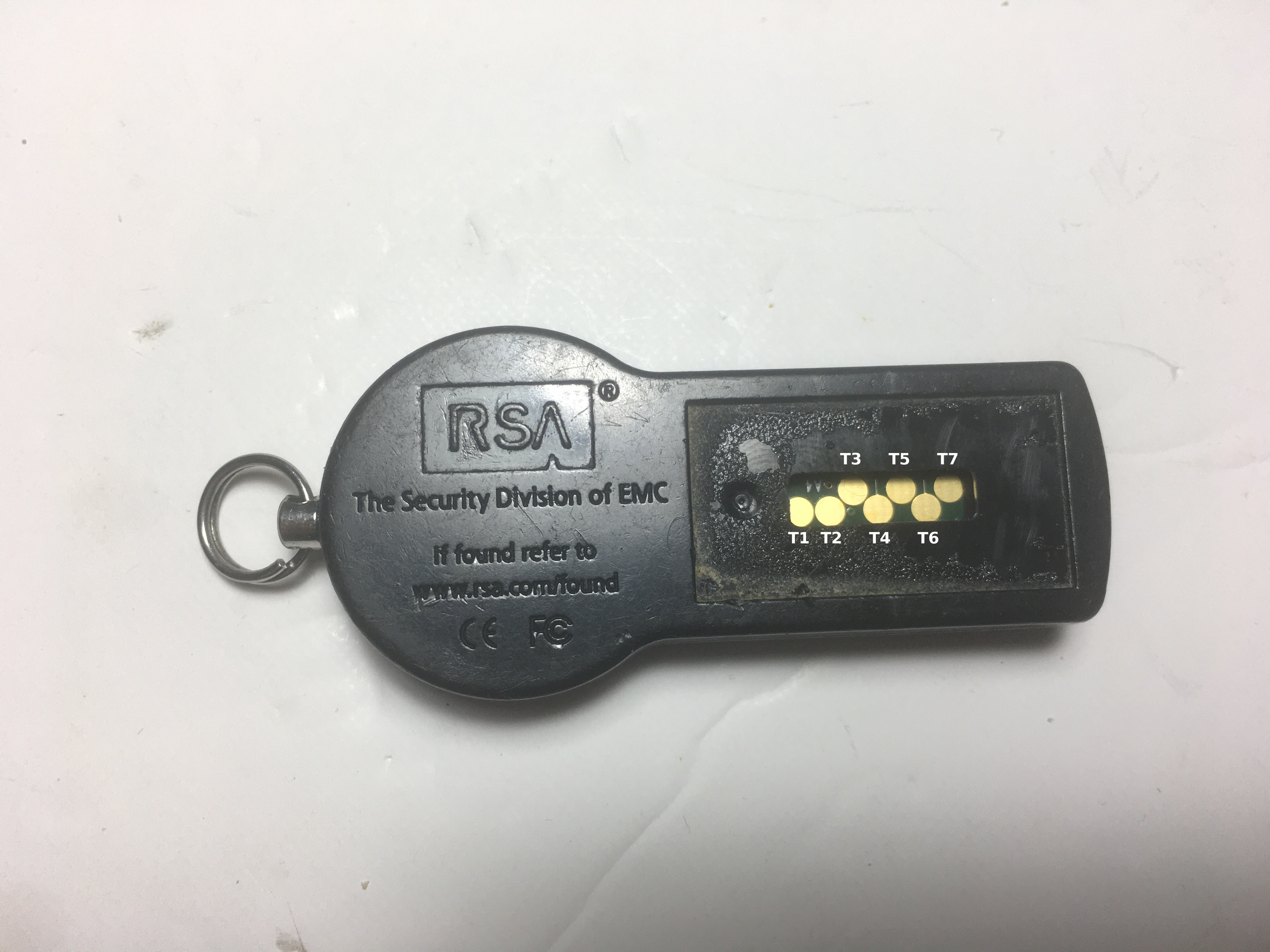
The serial number and expiration date of the token are printed on a piece of rubber on the back of the token that is easily removed to expose 7 circuit pads, an expensive arrangement if these pads are used just for testing as part of the manufacturer quality assurance process. Instead we believe that these pads are used to program the token with the seed.
This makes sense as the act of programming the seed into the token requires access to the secrets database to retrieve the serial and seed that the token needs to use, and to record the activation timestamp. It is likely that RSA would want to separate token manufacture from token “imprinting” given the very different security requirements for both processes.
With this in mind we believe that the manufacturing process would be split in two steps:
-
Assembly: Assemble the circuit and the physical token, likely in a standard fab facility. This step will include manufacturing the PCB, assembling the components, installing the battery and sealing the token. At this stage the token will be running without a seed.
-
Imprinting: Ship the tokens to a secure RSA facility where the token seeds are programmed using the 7 circuit pads and the serial number plus expiration dates are printed on the rubber cover and the imprinting time recorded in the central SecurID database.
The only sensitive component that would be exposed in step #1 would be the algorithm that would run inside the token, the microcontroller will probably have protections against extractions of the code - and in any event the algorithm is implemented in the soft tokens nowadays, so hardly a secret.
The cost of maintaining security in these separate scenarios would come at the expense of manufacturing efficiency, adding queueing between both facilities which probably explains the world-wide shortage of RSA tokens during COVID-19 due to the increased demand. You can easily ramp up assembly by using additional fabs, but the bottleneck would be the imprinting process as we assume there is a limited number of “imprinting” facilities.
Attacking the token
Hypothesis #1: Dump seed from EEPROM
Because the seed needs to be programmed at the time of imprinting, it needs to be stored somewhere where the microcontroller can access it, likely to be an EEPROM, maybe external to the microcontroller. It is possible that the data is somehow encrypted, but it will be great if we can extract it from the memory using something like eepeep. This is probably a naive assumption as the strength of the device depends on the security of the seed, but then again if we do not test the hypothesis we will never know.
To find out the location of the memory used to store the seed we need to disassemble the token and identify the components that make up the circuit - I used an expired token from my online banking (if you do not have one laying around you can get a batch of expired tokens off eBay).
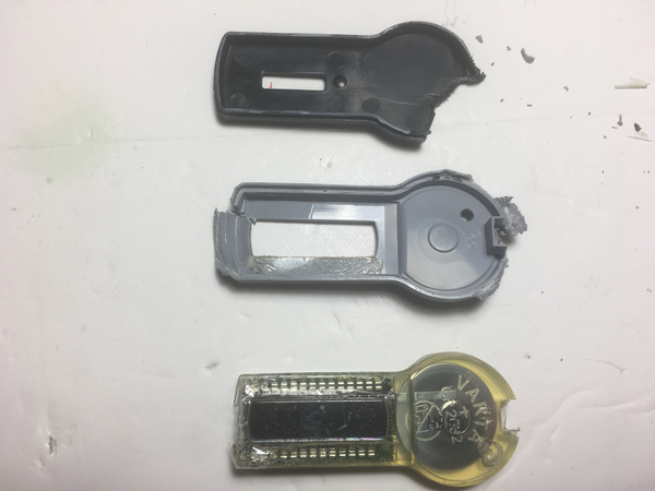
The external case of the token comes out quite easily, we just apply some force in the hole that the keyring holder is attached to and extract the circuit that is sandwiched between the top and bottom covers:
We can see that it uses a CR2032 3V battery to power the whole circuit, and the only visible areas are the 7 programming pads on one side (along with a few test pins and vias) and the LCD display on the other. The whole circuit is enclosed in semi-rigid transparent resin potting to waterproof the token. The removal of this resin is a matter of patience and exacto-knife and tweezers work, slowly cut into the resin and make sure you do not damage any of the components, then pull away chunks of resin using the tweezers.
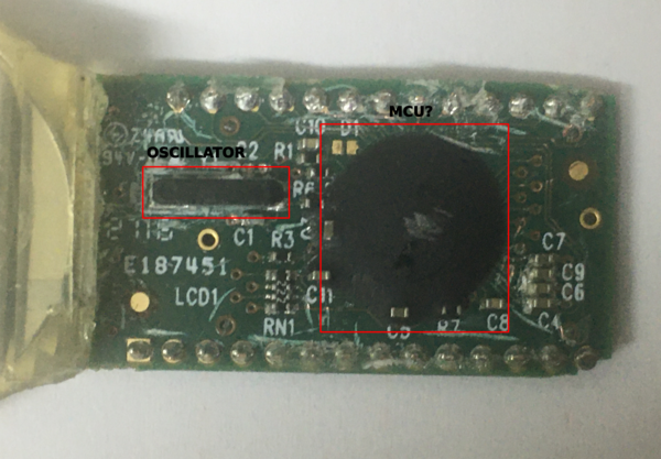
You will soon run out of resin and be left with the LCD display that hides the actual circuit so you can try to de-solder it or to pry it away with a screwdriver and a bit more of patience. With the LCD display removed we can see a few components, continue removing the resin (really carefully) until you get as much a clean as PCB as you can, something like this:
There are a couple of interesting markings on the PCB:
-
P/N 430P000012 REV A4, the part number and revision of this token design
-
E187451, a UL certificate for LEAD JUMP PCB (ZHUHAI) LTD, likely the fab used for the assembly of the token during the manufacturing process. The logo on the PCB also matches that of Lead Jump.
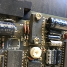
But that is about it, apart from a bunch of capacitors and resistors there appears to be only two active components:
-
An SMD oscillator: likely a 32.768KHz clock as used in real-time clock applications - markings on my oscillator are CB701, no datasheet identified.
-
An epoxy blob which seems to cover the MCU that drives the token.
No external EEPROM or any kind of memory, so the storage must be embedded as part of the MCU - no way to dump it using traditional methods, so let’s think of something else.
Hypothesis #2: Access memory using MCU pin functionality
For this attack attempt we need to understand the MCU architecture underneath the blob. Considering that RSA has manufactured close to 100 million of these devices and that the security of the device depends on the protection of the seed I expect this will be a custom die.
I do not have the lab equipment to remove the epoxy, x-ray the blob or de-layer the MCU so I looked for previous work undertaken in this area. I found the work by Travis Goodspeed who had exposed the MCU and done an initial analysis of the chip, however the resolution of the die images was too low so I could not look at the detail. Thanks to the contribution of Eduardo Cruz he located high-resolution images of the MCU put together by John McMaster.
Looking through the images I found work already done on reverse engineering the MCU in the siliconpr0n archives a few years ago. Going through the material I saw that they had identified a marking in the die “1C573718A” and that led them to the Sanyo LC573718A MCU, a general-purpose 4-bit MCU with some very familiar specs:
- Built-in LCD drivers to drive up to 120 segments (the SID700 SecurID token has a total of 49 LCD segments)
- Operates at 2.4V-3.6V
- Very low power consumption
- ROM: 8192 x 8 bits
- RAM: 512 x 4 bits
- Chronograph function with 100ms resolution
- Requires an external 32.768KHz oscillator and a bunch of capacitors
Funnily enough this MCU was originally created to run LCD games (it has a built-in buzzer port for instance). I could not find any references, but it will not be surprising if you found one powering a few Sanyo game watches.
At this stage it is impossible to know if Sanyo customised the MCU for RSA, however the pinout matches 100% that of the chip images (left image from Sanyo datasheet, right image SecurID die from siliconpr0n [credits]):
The datasheet is not very extensive, but it covers the pinout, which can be summarised as follows:
SEG1-SEG32 + COM1-COM4: LCD segment connectionsVDD1, VDD2, VDD3, VDDX, VSS, VSSX: Power connectionsXT1, XT2: Oscillator inputCUP1-CUP2: Capacitor pins for step-up, step-down (whatever this may be)P00, P01, P02, P03: 4-bit I/O portP10, P11: 2-bit I/O portM1, M2: 2-bit input portS1, S2, S3, S4: 4-bit input portALM: Buzzer output (it would be nice to have a bleeping fob)RES: ResetT3, TST, HZ32: Test pins
As we can see there are no references to pins to read/write from memory (or for in-system programming), so either the MCU does not have that capability to access and program memory or it is not documented on the datasheet.
A closer look at the MCU specs shows why there is no functionality to write into the MCU memory: the ROM is actually masked ROM which is written during the die manufacturing process by Sanyo, following RSA specs, and that cannot be modified at run-time. This means that all the tokens share the same ROM contents: static data and program code for the MCU but not the seed - as by the time the imprinting process happens the ROM can no longer be modified.
The only location where the seed can be stored is the MCU SRAM (!), a location that is wiped whenever the MCU loses power. But because the token is designed to constantly run on battery power the RAM is never wiped and the MCU holds the values stored there. If at any point the MCU loses power, the token loses the seed and it goes back to a pre-imprinting state (where the fob flashes with the “888888” message):
(While I was trying to free the old battery I managed to break the LCD, so only the unbroken segments flash - but you get the idea)
Because the SRAM is only accessible internally by the MCU there are no pins that expose its contents, so this attack cannot be progressed any more and the hypothesis needs to be abandoned.
Hypothesis #3: Extract the key from SRAM using die analysis
If the seed is stored in SRAM, can we not extract it directly from the die? Data stored in a SRAM is not optically visible, as each SRAM bit looks the same - to write and modify the bit a voltage is applied and a flip-flop is activated to hold the zero or the 1. Potentially and if you could remove the epoxy and chip cover without disconnecting the power supply you could use a SEM to measure voltage contrasts and systematically dump the contents of the SRAM.
While this sounds plausible this is well beyond my knowledge of electronics, so it is not a hypothesis that I could personally progress. Any comments, views or experiences on this welcome.
Hypothesis #4: Reverse engineer the imprinting process and use it to extract the seed instead of storing it
We have seen that the Sanyo MCU does not have any specific pins to access the SRAM, however this is not totally accurate for the RSA fobs: during the imprinting process the seed must be written to the SRAM using the 7 pads on the back of the token, so there are memory access capabilities through these external pads.
Let’s see if we can understand what each of the pads do and how they fit together to write the seed to the token - and then find out if the process can be used to read the seed back.
Quite a few hours of tracing with a multimeter show the following connections for the seven pad connectors (labelled from left to right):
T1: Ground?T2: Power?T3: Power / Reset?T4-T7: These four pins are connected through a 2.2k resistor network to the MCU. Because the connections go under the blob it is not possible to trace them easily, but judging from the pin positions and some of the MCU image pin usage these are likely to be connected to the M1, M2 (input only), P10 and P11 (input and output) ports.
These are GPIO pins whose functionality needs to be implemented in the ROM firmware by the developer of the particular application, in this case RSA. This means that the imprinting process does not use MCU native ports, but that the imprinting functionality is implemented in the firmware, so in order to understand what the pins do (and how the imprinting protocol works) we need to reverse engineer the firmware first.
Extracting the ROM using image processing
We go back to the previous work done by siliconpr0n who have really close-up images of the SecurID MCU available. As opposed to SRAM the mask ROM is static so it can be pre-programmed using fixed logical gate arrangements to store a zero or a one. There are various technologies for mask ROMs however with the appropriate decapping and staining it is possible to visually recognise when a zero or a one is stored on each memory position.
From the images we can see that there are 8KB of ROM organised in two banks. Each bank has 128 rows and each rows is 16 columns with 16 bits in each column, totalling 65536 bits (8 KB).
Using the images linked above and rompar, a masked ROM optical data extraction tool which takes an image of the masked ROM and produces the binary representation of the zeros and ones stored in it we were able to obtain the 8KB of the ROM that stores the configuration and program for the RSA token.
ROM structure
Now that we have the dump we need to try and make heads or tails of it, so that we can obtain the program running on the MCU. The main problem is understanding how the ROM is laid out, what part is the IC configuration and which part is the MCU program, so we can disassemble it.
At this point of time we would use the MCU documentation and development toolkit to compile a sample program, see how the data is stored and try to find patterns to understand how the masked ROM is created, however it seems that the age of this MCU coupled with the fact that Sanyo semiconductors has been resold multiple times leaves us with very little information and no working toolset to explore how the memory is laid down (if you happen to have access to such a toolkit drop me a line please).
During my research I have come across the following nuggets of information:
-
From the datasheets of the LC5734 family, LC573104A and LC573406A we have been able to extract the opcodes for the various instructions.
- From the similar LC65E1104_datasheet:
- Part of the mask ROM is the IC configuration, e.g. type of oscillator, watchdog reset, port output levels, etc. .
- The option data is stored between 0x1000 and 0x100a (10 bits)
- From the LC5862H datasheet:
- The option data is written to the end of the EPROM at 0x4000 to 0x40FF in blocks of 8 bits (256 bits)
I spent a considerable amount of time looking at the dump and the images to try and reverse-engineer the memory access method but it is just not my area of expertise. Looking at different permutations of the memory dump, coupled with a hand-made disassembler for the Sanyo MCUs did not bear any results so it seems like the memory layout is not straight-forward, the data is somehow encoded (e.g. RSA customised the chip to encode the instructions in the ROM, or the opcodes differ for this particular MCU). Considering that there are areas of memory with contiguous 1s or 0s, it does not seem like the encoding/encryption hypothesis holds up.
Completing the work
If you are successful in identifying the memory layout let me know, it should be a breeze afterwards to get the software decompiled and the imprinting process identified - as it stands though I need to abandon this avenue of work until there is a breakthrough in this area which will allow us to:
- Document how the imprinting process works
- Identify the SRAM addresses where the seed is written to
- Search for loopholes in the imprinting process to read back data from SRAM
Conclusion
We set ourselves to prove whether the hardware token seeds are substantially harder to compromise that soft tokens and, while there are still avenues for attack opened, it seems that the trust we put in hardware tokens is well-placed and that the design, although very surprising (seed stored in volatile RAM, non-dedicated IC), does hold itself to more than a casual effort at reverse engineering.
